Technology trends continue to drive miniaturisation in electronic components. As a result, product designers are often forced into specifying smaller and smaller devices on their bill of materials (BOM). Sometimes, miniature devices offer original equipment manufacturers (OEMs) cost savings, which is seen as a good thing; other times, there is simply no choice.
Component manufacturers continue to make devices obsolete in an attempt to release new technologies to market and keep up with consumer trends. This can be a problem for OEMs that have "old" versions of the part designed into their industrial hardware, as they may have to go through a redesign process.
Product designers are not always aware of the challenges redesigning their products to include miniature devices can cause. You could argue there is a disconnect between design and the manufacturing process. While electrically the new device may be fine, if it is located next to a much larger device then the electronics manufacturer may need to modify their build process and conduct additional trials to satisfy themselves they can consistently manufacture the product. All of which takes additional time and in some cases requires specialist equipment and tooling.
In this blog post, we share with you a case study featuring a printed circuit board assembly (PCBA) with a micro ball grid array (BGA) located next to a SIM card holder. We walk you through the process steps we took to ensure a consistent solder joint was made and share with you the results of the trials we conducted.
Unfortunately, we can’t tell you who the customer is. As with all our customers, we have a confidentially agreement in place but we can tell you they are a global security services company. We also can't tell you much about the product either, sorry. But we can tell you that the PCBA is doubled sided, 8up on a panel and includes a 0.4" pitch micro BGA (measuring 2.7mm x 2.4mm) located next to a SIM card reader measuring 26mm x 20mm, which is quite a difference.
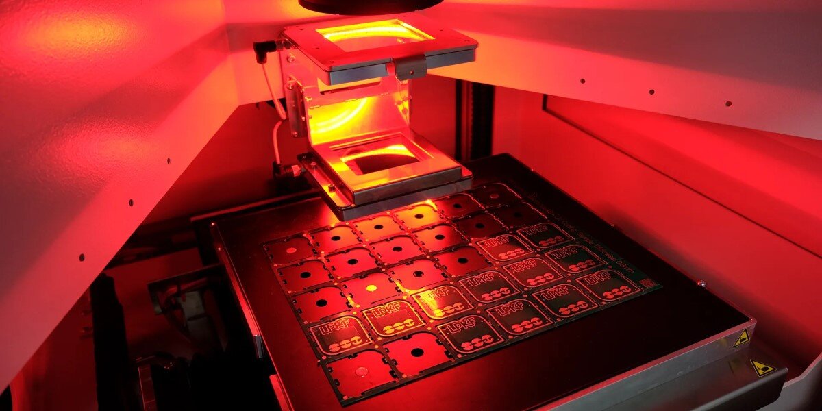
Multi-level solder stencil
This presented us with a challenge. The micro BGA would require a solder paste height of 0.08mm compared to the SIM card reader that would need 0.125mm. The conventional way to approach this particular challenge and achieve varying solder paste heights is to specify a multi-level solder stencil. There are two common techniques (stepped and additive) in creating multi-level stencils and if you would like to read more about the pros and cons of each we recently wrote a blog post covering this topic.
Unfortunately, after using a stepped stencil we identified solder shorts and an approximate 25 per cent failure rate on the micro BGA.
 Left image: BGA with shorts; right image: BGA without shorts
Although we felt it possible to make further improvements to the stencil material and design (change to electro-formed nickel with a reduced solder deposit and nano coating), we wanted to minimise the risk of shorts completely and decided to look into applying flux to the micro BGA directly.
Direct flux application
We trialled Mycronic's dip unit as it attached to our pick and place surface mount equipment. The unit consists of a squeegee and flux transfer plate, which has several cavities at different depths cut into it. Flux is dispensed and the squeegee then wipes it across the cavities leaving them filled, after which the micro BGA is picked and dipped directly into them.
During our trials, we built two panels consisting of 16 micro BGAs in total. We trialled two different flux depths and ran one panel with 0.1mm and the other with 0.14mm, with the aim of covering at least 50 per cent of the ball height (0.2mm) with flux. Too much flux can result in the part sticking in the cavity. There is also a danger that when it reflows the gaps between the balls become filled with flux residue which can be a problem if you need to make the joint stronger by underfilling with resin.
After the devices had been fitted to the board and reflowed, we re-inspected the boards to look for potential issues.
The results
We inspected the panels using X-ray, no shorts were found and we saw good placement. Although X-ray images can provide confidence and offer a good level of detail we always recommend several inspection methods when validating results.
 In order to make sure we were getting good wetting between the pad and the BGA, we decided to section one PCBA horizontally and the other vertically. Horizontal sectioning helped confirm the presence of good solder joints and it was possible to see where the ball had flowed around the pad separated by solder resist. In the vertical section, you can see that two balls have detached with the PCB pad still attached. For the purposes of our trial this wasn't a problem and occurred due to the forces applied during sectioning. To avoid this issue occurring again we would look to pot the PCB in a clear resin prior to sectioning.

Left image: horizontal section showing a slice through the centre of the BGA. You can also see the copper pad of the PCB, BGA ball and connection between both; right image: vertical section removing the device to leave just the solder balls
Our conclusions
Applying flux directly to micro BGAs is a good alternative to stencil printing but comes at a cost. Depending on the manufacturer a dip unit and transfer plate can cost anywhere between £13K-£17K, compared to a stepped stencil that typically costs just a few hundred pounds. Much depends on the products you are manufacturing and the quantities you intend to produce on a monthly basis. If the volumes are high enough then investment in an automated solution may well be the right decision for you. If, however, you are producing small batch quantities then you may not be able to justify the investment and need to continue trials with different stencil designs and materials.
Hopefully, this blog post has provided a useful insight into just one of the challenges electronics manufacturers face on a daily basis. Although the majority of issues can be overcome through robust engineering and NPI processes, the most effective way to mitigate them is to ensure design and manufacturing teams work closer from the outset.
So, if you're forced to make component changes in the future, we recommend you look at the rest of the board and then talk to your manufacturing partner before commiting to materials to ensure your design can be manufacturered in a cost-effective manner.
Image 1 by coniferconifer